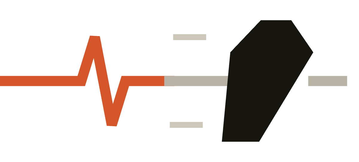
Buffer Layer

The take
You cannot force a technology into existence by throwing infinite capital at a bad foundation, meaning the cost of skipping the molecular buffer layer is watching your entire multi-billion-dollar semiconductor stack crack like dry mud under its own internal tension.
The Tell
Nature does not care about your venture capital runway. If the molecular foundation is mismatched, the whole stack cracks.

Stakes
Nature does not care about your venture capital runway or corporate R&D consensus. When trying to grow highly efficient gallium nitride on a cheap silicon base, the atomic mismatch is a physical reality that brute-force funding cannot bend; you either design a precise atomic runway to absorb the structural stress, or you build an expensive pile of microscopic gravel.
Source Dispatch
The read
For decades, corporate R&D giants like RCA Laboratories abandoned gallium nitride as an impossible dream, convinced that the material's structural defects were an engineering dead end.
Their executive consensus assumed that if a massive budget and scale could not brute-force the crystal growth, the science itself was flawed. They wanted the prize without the tedious, atomic-level negotiation.
In reality, the breakthrough did not come from a boardroom or a massive corporate subsidy, but from stubborn, isolated researchers who manually resolved the atomic dislocations.
By introducing an aluminum nitride buffer layer, they created a microscopic cushion that allowed mismatching crystal lattices to align without shattering. It was a triumph of material stoicism over administrative impatience.
This is the ultimate hardware reminder that some bottlenecks cannot be optimized away by agile sprints or infinite liquidity. When the foundation is physically mismatched, no amount of marketing or executive pressure can keep the stack from tearing itself apart.
The buffer layer is the quiet, unglamorous bridge that makes the high-voltage future possible.
In the wild
- The structural buffer needed to prevent hostile crystal substrates from cracking like dry mud during manufacturing.
- RCA Laboratories abandoning early GaN research due to insurmountable defect densities before buffer layer techniques were perfected.
- Dr. Umesh Mishra's pioneering work on GaN power transistors leveraging advanced nucleation and buffer layers.
- Episode: The High-Voltage Street Fight: Gallium Nitride's Power Transition (https://www.youtube.com/watch?v=srGmVOFpasU)
- A buffer layer! I like the word buffer.
Related
 AI SlopPlatforms pay for volume, so the machine floods your feed with filler until the real stuff drowns. That sludge is AI slop.
 SaaspocalypseThe joke stopped being a joke. Vibe-coded custom tools are eating the monthly SaaS stack one workflow at a time. That slaughter is Saaspocalypse.
 Vibe CodingVibe coding was sold as everyone becoming a software mogul. What it actually does is liquidate entry-level coding jobs and leave the high-agency architect as the only adult in the room who can debug the beautiful mess a model spat out in three seconds.
 Terminally onlineTerminally Online is when the feed's stakes feel more real than your actual life. Likes, outrage loops, and timeline drama become the OS; IRL is the side quest.
 NewsjackNewsjacking is when a brand or influencer hijacks a trending news story or event to promote their own sh*t. Basically the digital equivalent of an ambulance chaser, but for clicks.
 Long ElectronsSilicon Valley wants you to believe AI is a pure software miracle trading at infinite multiples, but going Long Electrons is the hard macro pivot that exposes the risk of investing in paper intelligence while ignoring the decaying physical grid that actually powers it.
Gifnotes poster
Sources
FAQ
What is a buffer layer in semiconductor manufacturing?
It is an intermediate material grown between a substrate and an active semiconductor layer to absorb structural and thermal mismatches. Without this atomic cushion, the lattice differences between materials like gallium nitride and silicon cause the top layer to crack, rendering the chip useless.
Why did early corporate R&D fail to commercialize gallium nitride?
Conglomerates like RCA tried to brute-force gallium nitride growth directly onto mismatched substrates using massive budgets but ignoring the atomic stress. They abandoned the material as a dead end, failing to realize that nature requires a physical buffer layer to negotiate the molecular tension.
How does an AlN buffer layer solve the structural mismatch?
An aluminum nitride (AlN) buffer layer acts as a transitional atomic runway. It bridges the physical gap between the silicon substrate and the gallium nitride layer, absorbing the dislocation defects and thermal stress so the high-performance crystal can grow smoothly.
Who actually solved the gallium nitride buffer layer bottleneck?
Isolated, persistent researchers in Japan and later pioneers like Dr. Umesh Mishra worked through the tedious materials science of low-temperature buffer layers. Their manual, methodical engineering succeeded where massive, impatient corporate R&D programs had surrendered.